Visit
to a PCB fabricator
home>gallery>pcb fabricator
I
designed a PCB for a robotics workshop held in our college
recently. We needed 20 PCBs in all, so we decided to get them
fabricated at a local pcb fabricator in the suburbs. I jumped
on the opportunity to capture the whole pcb fabrication process
on camera.
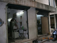
The
fabricator's setup was typical by Indian standards. It looked
chaotic at first sight, but as usual, there was order in disorder.
Although it wouldn’t be right for me to comment on the
working conditions, I can sum it up in one word - "pathetic".
The owner was friendly and gave us a small walk-through of
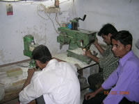
the entire process. The shop was primarily divided into two
sections, one was the mechanical, where cutting, drilling
and polishing took place while in the other half, printing,
etching and tinning was done.
The whole process starts with cutting of copper clad boards
into appropriate sizes. Parallely, a screen is prepared for
'printing' the pcb pattern on the boards. It’s an usual
screen printing process.
1. A negative is developed from the pcb layout
2. A positive layout is then developed on a printing screen,
which consists of a finely woven fabric.
3. The pattern is then printed on the pcb by placing it under
the screen and applying the colour over it.
4. The printed board is then dried in an oven.
5. Now the board is etched using ferric chloride solution
in an etching tank.
6. After etching the board is washed
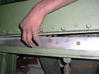
7. Holes are then drilled (one at a time - the most time consuming
process of all )
8. The PCBs are polished using a steel wool
9. If necessary, solder mask is applied using the same screen
printing technique
10. The board is tinned
The PCB is now complete and ready to ship!
click to enlarge:-
PCBs
being cut into required sizes |
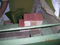
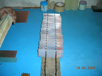
Stack
of pre cut PCBs |
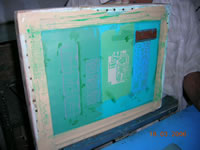
The
developed screen |
| 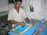
Application
of colour on the screen, (screen printing) |
The
printed pcbs are left to dry on a nail stand |
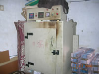
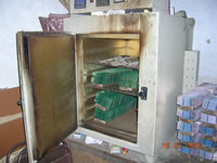
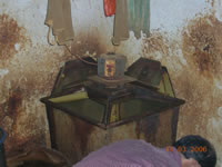
The
oven |
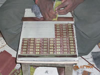
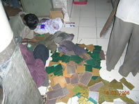
You
can see the pcbs with and without solder mask |
Etching
tank, most hazardous place of all ! |
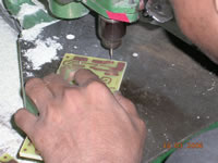
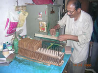
Drilling |
There
were in all four small drill press in this shop |
The
PCBs are polished before tinning. |
Application
of the solder mask |
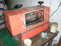
The
tinning machine consists of a rotating roller dipped
in molten solder |
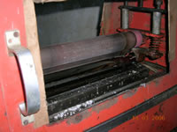
A
close up |
The
finished PCBs being cleaned |
|
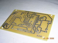
Our
PCB ! |
|
28
march 2006